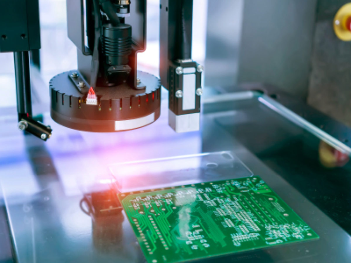
There are a lot of factors that affect the quality of PCBA. It’s important to understand what these factors are so that you can maintain high quality standards. This article will help you determine where and how to inspect your PCB Assembly line so that you can deliver the best product possible while keeping costs low and efficiency high.
Is the solder mask continuous over the entire surface?
The solder mask is the green layer that covers the copper traces. It is important to make sure that it is continuous over the entire surface of each board, because if there are any gaps in its coverage it could cause a short circuit and/or be a potential source of contamination.
Are there any local breaks in the copper patterns?
When inspecting your PCB, you should check for any local breaks in the copper patterns. A break in the copper pattern can be caused by a faulty component or a problem with the PCB itself. If there are any local breaks in your PCB circuit board, it may affect its performance.
Is any copper pattern absent or incorrectly positioned?
This is a fairly straight forward inspection. You can check for missing or misaligned pads, vias, holes, plated through holes, and power and ground traces.
Are all SMD resistors & capacitors correctly aligned and placed within the tolerance allowance of 0.5 mm?
Are all SMD resistors and capacitors correctly aligned and placed within the tolerance allowance of 0.5 mm? Are there any solder bridges, solder balls or missing components?
Related: UI/UX Design
Check for pinholes, cracks and other visible defects on the solder mask.
Check for pinholes, cracks and other visible defects on the solder mask.
This is done on both sides of the board. Then you can check for any missing or misaligned pads, vias, holes, plated through holes and power and ground traces. This is done on both sides of the board. You can check for missing or misaligned pads, vias, holes, plated through holes and power and ground traces.
Check for scratches, pinholes and other visible defects on the silk screen.
Inspect the surface of the solder mask for any visible defects, including cracks and pinholes. Inspect the silk screen for any visible damage or defects. If there are visible defects, the PCB assembly should be reballed. This will ensure that the board is repaired properly and ready for service. If the board passes all of these tests, it’s ready for testing and assembly.
Conclusion
As you can see, there are quite a few things to check when it comes time for your PCB assembly inspection. It can be difficult to ensure that all of these checks have been made correctly, but with the right tools and knowledge, it’s possible! When in doubt about any aspect of your PCB assembly inspection checklist or process, don’t hesitate to contact the service providers. They will be able to help you stay on top of your PCB assembly inspection checklist so that you can ensure that your boards are ready for service.


